In this chapter, you will learn the following:
Clocks: Covers clocks, clock signals, and the key components of clocks.
Time error: Explains what time error is, the different types of metrics to quantify time error, and how these metrics are useful in defining clock accuracy and stability.
Holdover performance: Explains holdover for clocks, applicable whenever a synchronization reference is temporarily lost, and why the holdover capability of a clock becomes critical to ensure optimal network and application functioning.
Transient response: Examines what happens when a slave clock changes its input reference.
Measuring time error: Describes how to determine and quantify the key metrics of time error.
In earlier chapters, you read that any clock can only be near perfect (none are perfect)—there are always inherent errors in clocks. In this chapter, you will discover the various components of a clock and understand how these components contribute to removing or introducing certain errors. Because these errors can adversely impact the consumer of the synchronization services (the end application), it is important to track and quantify them. Once measured, these errors are compared against some defined performance parameters to determine how much (if any) impact they have on the end application. This chapter also explains the different metrics used to quantify time error and how to measure them.
Clocks
In everyday usage, the term clock refers to a device that maintains and displays the time of day and perhaps the date. In the world of electronics, however, clock refers to a microchip that generates a clock signal, which is used to regulate the timing and speed of the components on a circuit board. This clock signal is a waveform that is generated either by a clock generator or the clock itself—the most common form of clock signal in electronics is a square wave.
This type of clock is able to generate clock signals of different frequencies and phases as may be required by separate components within an electronic circuit or device. The following are some examples showing the functions of a clock:
Most sophisticated electronic devices require a clock signal for proper operation. These devices require that the clock signal delivered to them adheres to a core set of specifications.
All electronics devices on an electronic circuit board communicate with each other to accomplish certain tasks. Every device might require clock signals with a different specification; providing the needed signals allows these devices to interoperate with each other.
In both cases, a clock device on the circuit board provides such signals.
When discussing network synchronization or designing a timing distribution network, the timing signals need to travel much further than a circuit board. In this case, nodes must transfer clock signal information across the network. To achieve this, the engineer designates a clock as either a master clock or a slave clock. The master clock is the source for the clock signals, and a slave clock then synchronizes or aligns its clock signals to that of the master.
A clock signal relates to a (hardware) clock subsystem that generates a clocking signal, but often engineers refer to it simply using the term clock. You might hear the statement, “the clock on node A is not synchronized to a reference clock,” whereas the real meaning of clock in this sentence is that the clock signals are not synchronized. So, clock signal and clock are technically different terms with different meanings, but because the common usage has made one refer to the other, this chapter will also use the term clock to refer to a clock signal.
Oscillators
An electronic oscillator is a device that “oscillates” when an electric current is applied to it, causing the device to generate a periodic and continuous waveform. This waveform can be of different wave shapes and frequencies, but for most purposes, the clock signals utilized are sine waves or square waves. Thus, oscillators are a simple form of clock signal generation device.
There are a few different types of oscillators (as described in Chapter 3, “Synchronization and Timing Concepts”), but in modern electronics, crystal oscillators (referred to as XO) are the most common. The crystal oscillator is made up of a special type of crystal, which is piezoelectric in nature, which means that when electric current is applied to this crystal, it oscillates and emits a signal at a very specific frequency. The frequency could vary from a few tens of kHz to hundreds of MHz depending on the physical properties of the crystal.
Quartz is one example of a piezoelectric crystal and is commonly used in many consumer devices, such as wristwatches, wall clocks, and computers. Similar devices are also used in networking devices such as switches, routers, radio base stations, and so on. Figure 5-1 shows a typical crystal commonly utilized in such a device.
)

Figure 5-1 16-MHz Crystal Oscillator
The quartz that is being used in crystal oscillators is a naturally occurring element, although manufacturers grow their own for purity. The natural frequency of the clock signal generated by a crystal depends on the shape or physical properties (sometimes referred to as the cut) of the crystal.
On the other hand, the stability of the output signal is also heavily influenced by many environmental factors, such as temperature, humidity, pressure, vibration, and magnetic and electric fields. Engineers refer to this as the sensitivity of the oscillator to environmental factors. For a given oscillator, the sensitivity to one factor is often dependent on the sensitivity to another factor, as well as the age of the crystal or device itself.
As a real-life example, if your wristwatch is using a 32,768-Hz quartz crystal oscillator, the accuracy of the wristwatch in different environmental conditions will vary. The same behavior also applies to other electronic equipment, including transport devices and routers in the network infrastructure. This means that when electronic devices are used to synchronize devices to a common frequency, phase, or time, the environmental conditions adversely impact the stability of synchronization.
There have been many innovations to improve the stability of crystal oscillators deployed in unstable environmental conditions. One common approach in modern designs is for the hardware designer to design a circuit to vary the voltage being applied to the oscillator to adjust its frequency in small amounts. This class of crystal oscillator is known as voltage-controlled crystal oscillators (VCXO).
Of the many environmental factors that affect the stability and accuracy of a crystal oscillator, the major one is temperature. To provide better oscillator stability of crystal against temperature variations, two additional types of oscillators have emerged in the market:
Temperature-compensated crystal oscillators (TCXO) are crystal oscillators designed to provide improved frequency stability despite wide variations in temperature. TCXOs have a temperature compensation circuit together with the crystal, which measures the ambient temperature and compensates for any change by altering the voltage applied to the crystal. By aligning the voltage to values within the possible temperature range, the compensation circuit stabilizes the output clock frequency at different temperatures.
Oven-controlled crystal oscillators (OCXO) are crystal oscillators where the crystal itself is placed in an oven that attempts to maintain a specific temperature inside the crystal housing, independent of the temperature changes occurring outside. This reduces the temperature variation on the oscillator and thereby increases the stability of the frequency. As you can imagine, oscillators with additional heating components end up bulkier and costlier than TCXOs.
The basic approach with the TCXO is to compensate for measured changes in temperature by applying appropriate changes in voltage, whereas for the OCXO, the temperature is controlled (by being elevated above the expected operating temperature range). Figure 5-2 shows a typical OCXO.
)
Figure 5-2 Typical OCXO
An oscillator is the core component of a clock, which alone can significantly impact the quality of the clock. An approximate comparison of stability between these different oscillators suggests that the stability of an OCXO might be 10 to 100 times higher than a TCXO class device. Table 3-2 in Chapter 3 outlines the characteristics of the common types of oscillator.
The stability of an oscillator type also gets reflected in the cost. As a very rough estimate, cesium-based oscillators cost about $50,000 and rubidium-based oscillators around $100, whereas an OCXO costs around $30 and a TCXO would be less than $10.
PLLs
A phase-locked loop (PLL) is an electronic device or circuit that generates an output clock signal that is phase-aligned as well as frequency-aligned to an input clock signal. As shown in Figure 5-3, in its simplest form, a PLL circuit consists of three basic elements, as described in the list that follows.
)
Figure 5-3 PLL Building Blocks
Voltage-controlled oscillator (VCO): A special type of oscillator that changes frequency with changes in an input voltage (in this case from the loop filter). The frequency of the VCO with a nominal control signal applied is called the free-running frequency, indicated by the symbol f0.
Phase comparator: Compares the phase of two signals (input clock and local oscillator) and generates a voltage according to the phase difference detected between the two signals. This output voltage is fed into the loop filter.
PLL loop filter: Primary function is to detect and filter out undesired phase changes passed on by the phase comparator in the form of voltage. This filtered voltage is then applied to the VCO to adjust the frequency. It is important to note that if the voltage is not filtered appropriately, it will result in a signal that exactly follows the input clock, inheriting all the variations or errors of the input clock reference. Thus, the properties of the loop filter directly affect the stability and performance of a PLL and the quality of the output signal.
When a PLL is initially turned on, the VCO with a nominal control signal applied will provide its free-running frequency (f0). When fed an input signal, the phase comparator measures the phase difference compared to the VCO signal. Based on the size of the phase difference between the two signals, the phase comparator generates a correcting voltage and feeds it to the loop filter.
The loop filter removes (or filters out) the noise and passes the filtered voltage to the VCO. With the new voltage applied, the VCO output frequency begins to change. Assuming the input signal and VCO frequency are not the same, the phase comparator sees this as a phase shift, and the output of the loop filter will be an increasing or decreasing voltage depending on which signal has higher frequency.
This voltage adjustment causes the VCO to continuously change its frequency, reducing the difference between VCO and input frequency. Eventually the size of changes in the output voltage of the loop filter are also reduced, resulting in ever smaller changes to the VCO frequency—at some point achieving a “locked” state.
Any further change in input or VCO frequency is also tracked by a change in loop filter output, keeping the two frequencies very closely aligned. This process continues as long as an input signal is detected. The filtering process is covered in detail in the following section in this chapter.
Recall that the input signal, even one generated from a very stable source (such as an atomic clock), would have accumulated noise (errors) on its journey over the clocking chain. The main purpose of a PLL is to align frequency (and phase) to the long-term average of the input signal and ignore (filter out) short-term changes.
Now a couple of questions arise:
Will the loop filter react and vary the voltage fed to the VCO for every phase variation seen on the input signal?
When should the PLL declare itself in locked state or, conversely, if already in locked state, under what conditions could the PLL declare that it has lost its lock with the input reference?
The first question raised is answered in the next section, but the second question needs a discussion on PLL states and the regions of operation of a PLL. The PLL is said to be in the transient state when the output is not locked to the input reference and it is in the process of locking to the input signal. Alternatively, the steady state is when the PLL is locked with the input reference. As explained earlier, even during steady-state operations, the VCO will keep adjusting the frequency to match the input frequency based on the differential voltage being fed from the loop filter.
These states are governed by three different frequency regions, known as hold-in range, pull-in range, and pull-out range. Figure 5-4 illustrates these frequency ranges.
)
Figure 5-4 Frequency Ranges of PLL Operations
These frequency ranges are always quoted relative to the free-running frequency of the VCO (f0) and are specified in parts per million (ppm) or parts per billion (ppb). Because these are ranges, there needs to be both minimum and maximum values. If not explicitly specified, the range is interpreted as including everything between the positive and negative values of the specified number. For example, if the range is specified as 4.6 ppm (or 4.6 × 10⁻⁶), the range is assumed to cover a range between –4.6 ppm and +4.6 ppm around f0.
As per ITU-T G.810, the definitions of these frequency regions are as follows:
Hold-in range: “The largest offset between a slave clock’s input signal and the nominal (natural) frequency of its VCO, within which the slave clock maintains lock as the frequency varies arbitrarily slowly over the frequency range.”
This is the range of difference between the nominal frequency and input frequency for which the PLL can steadily maintain phase tracking while in a steady (or locked) state. If the frequency of the input reference is slowly reduced or increased within the range, the PLL can still track it. The edge of the hold-in range is the point at which the PLL will lose the locked state.
Pull-in range: “The largest offset between a slave clock’s input signal and the nominal (natural) frequency of its VCO, within which the slave clock will achieve locked mode.”
This is the range of difference between the nominal frequency and the input frequency for which the PLL will always become locked throughout an acquisition (or tracking) process. Note that during this acquisition process there might be more than one cycle slip, but the PLL will always lock to the input signal. This is the range of frequencies within which a PLL can transition from the transient state to steady (locked) state.
Pull-out range: “The offset between a slave clock’s input signal and the nominal (natural) frequency of its VCO, within which the slave clock stays in the locked mode and outside of which the slave clock cannot maintain locked mode, irrespective of the rate of the frequency change.”
This can be seen as the range of the frequency step, which if applied to a steady-state PLL, the PLL still remains in the steady (or locked) state. The PLL declares itself not locked if the input frequency step is outside of this range.
Taking an example from ITU-T G.812, both the pull-in and hold-in ranges for Type III clock type is defined as 4.6 × 10⁻⁶, which is the same as ±4.6 ppm. Table 3-3 in Chapter 3 provides a quick reference of these frequency ranges for different types of clock nodes.
When the PLL is tracking an input reference, it is the loop filter that is enforcing the limits of these frequency ranges. The loop filter is usually a low-pass filter, and as the name suggests, it allows only low-frequency (slow) variations to pass through. That means it removes high-frequency variation and noise in the reference signal. Conversely, a high-pass filter allows high-frequency variations to pass and removes the low-frequency changes.
While these filters are discussed in the next section in detail, it is important to note that “low-frequency variations” does not refer to the frequency of the clock signal, but the rate with which the frequency or phase of the clock signal varies. Low rate (less frequent) changes are a gradual wander in the signal, whereas high rate changes are a very short-term jitter in the signal. You will read more about jitter and wander later in this chapter.
Because PLLs synchronize local clock signals to an external or reference clock signal, these devices have become one of the most commonly used electronic circuits on any communication device. Out of several types of PLL devices, one of the main types of PLL used today is the digital PLL (DPLL), which is used to synchronize digital signals.
It is worthwhile noting that, just like any other electronic circuits and devices, PLLs have also been evolving. Designers of modern communications equipment are incorporating the latest PLL devices into them, circuits that now contain multiple PLLs (analogue or digital).
To reduce real-estate requirements on circuit boards, newer-generation devices can operate with lower-frequency oscillators that can replace expensive high-frequency oscillators. They also output signals with ultra-low levels of jitter that is required for the tight jitter specifications required by some equipment designs (remembering that jitter is high-frequency noise).
Low-Pass and High-Pass Filters
A low-pass filter (LPF) is a filter that filters out (removes) signals that are higher than a fixed frequency, which means an LPF passes only signals that are lower than a certain frequency—hence the name low-pass filter. For the same reasons, sometimes LPFs are also called high-cut filters because they cut off signals higher than some fixed frequency. Figure 5-5 illustrates LPF filtering where signals with lower frequency than a cut-off frequency are not attenuated (diminished). The pass band is the range of frequencies that are not attenuated, and the stop band is the range of frequencies that are attenuated.
Meanwhile, the range up to the cut-off frequency becomes the clock bandwidth, which also matches the width of a filter’s pass band. For example, as shown in Figure 5-5, in the case of an LPF, the clock bandwidth is the range of frequencies that constitute the pass band. The clock bandwidth is typically a configurable parameter based on the capabilities of a PLL.
)
Figure 5-5 Low-Pass Filter
Similarly, a high-pass filter (HPF) is a device that filters out signals that are lower than some fixed frequency, which means that an HPF passes only signals that are higher than a certain frequency. And again, HPFs are also sometimes called low-cut filters because they cut off lower than a fixed frequency signal. Figure 5-6 depicts an HPF, showing that the pass band and stop band are a mirror image of the LPF case.
)
Figure 5-6 High-Pass Filter
It is interesting to note that combining both filters (LPF and HPF) on a circuit, you could design a system to allow only a certain range of frequencies and filter out the rest. Such a combination of LPF and HPF behaves as shown in Figure 5-7 and is called a band-pass filter. The band-pass name comes from the fact that it allows a certain band of frequencies (from lower cut-off to higher cut-off) to pass and attenuates the rest of the spectrum.
)
Figure 5-7 Band-Pass Filter
These filters are of the utmost importance when trying to filter errors out from a clock signal. To understand this process in more detail, this chapter next defines these errors, primarily jitter and wander, more technically.
Jitter and Wander
Jitter and wander are phase variations in the clock signal timing instants, as illustrated in Figure 5-8. Also, refer to the introduction to jitter and wander in Chapter 3. This variance and error, commonly called clock signal noise, can be caused by many factors, one being the quality of the clock components. Another factor is the noise accumulating from one node to the next when distributing timing signals through a chain of clocks.
)
Figure 5-8 Jitter Versus Ideal Versus Wander
Low rate (less frequent, slower) changes are a gradual wander in the signal, whereas high rate changes are a very short-term jitter in the signal. The ITU-T specifies (in G.810) that 10 Hz is the dividing line between jitter and wander (and has been a convention in the telecom industry for some time). And so, phase variations occurring at rate higher than 10 Hz are described as jitter, and the variations lower than 10 Hz are described as wander.
When all the phase variations of a clock signal as compared to its reference signal are measured and plotted in a graph, for jitter the resultant frequency (or rate) of the phase variations is higher than 10 Hz (ten variations per second). Figure 5-9 shows one such example of jitter, where the y-axis shows the phase variations (in ns), and the x-axis shows the time of variation (in seconds) itself. As depicted in Figure 5-9, the rate of phase variations recorded is much higher than 10 Hz, and such phase variations are classified as jitter.
)
Figure 5-9 Plot of Phase Deviations Showing Jitter in a Clock Signal
For wander, in a similar approach, a graph plotting the phase variations will show the frequency (or rate) of less than 10 Hz. It is important to note that the rate of phase variations for wander could go down to mHz or μHz (rate down to once in several minutes or hours). For this reason, it is always recommended to run wander measurement tests for long periods of time (hours or days).
As you read in Chapter 3, the jitter (and wander to some extent) can be filtered out, and to do that, filters are used. If one configures an LPF with 10 Hz as the cut-off frequency, it will eliminate phase variation with a rate of variation higher than 10 Hz. Because jitter is defined as phase variation above 10 Hz, any LPF configured this way filters out jitter.
Similarly, an HPF configured with a 10-Hz cut-off will filter out wander, because the HPF will filter out variations with a rate of 10 Hz or lower.
Phase variations from a real-life test are captured in Figure 5-10, Figure 5-11, and Figure 5-12, which show, respectively: 1) phase deviations of a clock signal with jitter and wander present with no filter; 2) with an HPF filter applied; and 3) with an LPF filter applied. In these figures, the y-axis shows phase variations (in ns), and the x-axis shows the time elapsed since the measurement was started (in minutes).
The graph shown in Figure 5-10 captures all the phase variations of a clock signal (low and high rate phase variations plotted in a single graph), and so it is not easy to visualize the jitter and the wander of a clock signal.
)
Figure 5-10 Plot of Phase Deviations of a Clock Signal Without Any Filters
In order to clearly visualize (and analyze) the jitter and wander, filters are applied to the phase variation measurements. In Figure 5-11, you can see that after the HPF is applied (which filters out the wander), the remaining noise is jitter (frequency of phase variations higher than 10 Hz).
)
Figure 5-11 Plot of Phase Deviations of a Clock Signal After HPF Applied
Similarly, in Figure 5-12, after the LPF is applied (which filters out the jitter), the remaining noise is wander.
)
Figure 5-12 Plot of Phase Deviations of a Clock Signal After LPF Applied
After reading the preceding section about clock bandwidth and the PLL loop filter, there are two questions that could arise. First, why not keep the LPF cut-off frequency very low to filter the jitter and also limit the wander? Recall that jitter is filtered with the LPF. And if the LPF cut-off frequency is kept low, it could also filter some range of wander. Of course, this means that the pass band for the LPF becomes very small. Secondly, why not do the same on every clock node in the chain?
To understand the answer to the second question, you first need to appreciate the following aspects of PLLs:
Not all PLLs can keep LPF cut-off frequency very low. Wander is classified as low-rate phase variations, which can reach extremely small values—10 Hz down to microhertz. So, there will always be some phase noise (in this case wander) within the LPF clock bandwidth and so will always be tracked by the PLL.
A PLL combines two signals: 1) the input reference signal and 2) the clock signal from the local oscillator (VCO) to output a synchronized signal. When the PLL loop filter (LPF) blocks the signal from the input reference, the output signal is constructed using the local oscillator.
So the process of a PLL filtering the noise from the input signal is substituting noise from the local oscillator. Taken to a theoretical corner case, if the clock bandwidth of an LPF is made zero, all that the PLL will output is the signal from the local oscillator—which defeats the purpose of having a reference signal.
So, if using a very low cut-off frequency for the LPF, the PLL needs to be matched to a good-quality local oscillator, so that the noise added by the local oscillator is reduced. For the hardware designer, this has obvious cost ramifications—to get better noise filtering, you need to spend more money on the oscillator.
The time taken for a PLL to move from transient state to the steady (or locked) state depends on the clock bandwidth (as well as the input frequency and quality of the local oscillator). The narrower the clock bandwidth for the LPF, the longer time it takes for the PLL to move to the steady state.
For example, a synchronization supply unit (SSU) type I clock or building integrated timing supply (BITS) stratum 2 clock with an LPF configured for bandwidth of 3 mHz will take several minutes to lock to an input signal. However, telecom networks are very widely distributed and can consist of long chains of clock nodes. If all the clocks in the chain had low bandwidth, the complete chain could take many hours to settle to a steady state. Similarly, it might take several hours for the last node of the chain to settle down after any disruption to the distribution of clock.
It is for these reasons that a clock node with better filtering capabilities should have a good-quality oscillator and should be placed in a chain of clock nodes at selected locations. These factors also explain why SSU/BITS clock nodes (which have stratum 2–quality oscillators and better PLL capabilities) are recommended only after a certain number of SDH equipment clock (SEC) nodes. The section “Synchronization Network Chain” in Chapter 6, “Physical Frequency Synchronization,” covers this limit and recommendations by ITU-T in greater detail.
To ensure interoperability between devices and to minimize the signal degradation due to jitter and wander accumulation across the network, the ITU-T recommendations (such as G.8261 and G.8262) specify jitter and wander performance limits for networks and clocks. The normal network elements (NE) and synchronous Ethernet equipment clocks (EEC) are usually allocated the most relaxed limits.
For example, ITU-T G.8262 specifies the maximum amount of peak-to-peak output jitter (within a defined bandwidth) permitted from an EEC. This is to ensure that the amount of jitter never exceeds the specified input tolerance level for subsequent EECs. Chapter 8, “ITU-T Timing Recommendations,” covers the ITU-T recommendations in greater detail.
Frequency Error
While jitter and wander are both metrics to measure phase errors, the frequency error (or accuracy) also needs to be measured.
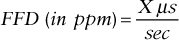
The frequency error (also referred to as frequency accuracy) is the degree to which the frequency of a clock can deviate from a nominal (or reference) frequency. The metric to measure this degree is called the fractional frequency deviation (FFD) or sometimes just the frequency offset. This offset is also referred to as the fractional frequency offset (FFO).
The basic definition is given in ITU-T G.810 by the following equation:

where:
y(t) is the FFD at time t
v(t) is the frequency being measured and
vnom is the nominal (or reference) frequency
FFD is often expressed in parts per million (ppm) or parts per billion (ppb). For example, the free-running frequency accuracy of a synchronous Ethernet (SyncE) clock is < 4.6 ppm, while the carrier frequency accuracy required in cellular mobile radio is < 50 ppb.
Taking an example calculation, if the nominal frequency of an oscillator is 20 MHz (which is 20,000,000 Hz and represents vnom as per the previous ITU-T G.810 formula) and the measured frequency is 20,000,092 Hz, then the FFD for this case (in ppm) will be

Using the same formula, a measured frequency of 19,999,08 Hz and nominal frequency of 20,000,000 Hz will give the FFD as –4.6 ppm.
FFD can also be expressed in units of time. For example, an FFD of +4.6 ppm means that the measured signal is accumulating 4.6 μs of time for each second, whereas an FFD of +4.6 ppm means that the measured signal is losing 4.6 μs of time for each second. After 10 s of real time, the signal would be off by 46 μs compared to the reference signal. This is known as the frequency drift and the relation is as follows:
ITU-T clock specifications such as ITU-T G.812, define the holdover specification (also called long-term transient response) using frequency accuracy. This sets the limits of the drift of a clock away from the frequency to which it was previously locked. Also, other ITU-T clock specifications, such as ITU-T G.813, define the frequency accuracy of the free-running clock. This defines the required accuracy of the frequency of a clock at start-up, before it has been locked to any other reference.